Nothing in the ordinary world informs our intuition about how materials will behave at molecular interfaces. The cartoon below shows a typical imprinting process: a photoimageable imprint resin formed into a layer on a rigid substrate (silicon or glass wafer), with the PDMS (silicone) mold hovering above. You lower the PDMS mold into the resin to make the imprint, flash the UV lamp to cure the resin, and lift off the PDMS mold.
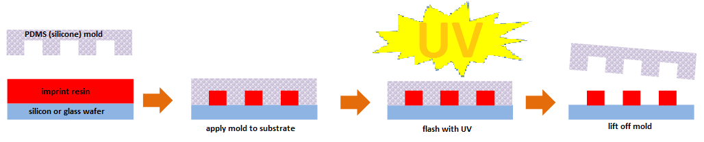

You want the cured resin to have good adhesion to the substrate, to separate cleanly from the PDMS mold, and leave behind a perfect imprint of the mold in the cured resin. But we’ve all had the experience of unmolding something, only to find some part of what we are molding stuck to the mold, and the corresponding piece missing from our molded object.
This has a lot to do with adhesion, of which there are many different mechanisms that are applicable to different materials and situations. With the ever shrinking dimensions of imprinted devices, surface effects and atomic contact between different materials become major considerations.
Some of the mechanisms that help to explain the behavior of materials at interfaces include:
Mechanical – Material A fills the cracks or pores of the surface of Material B and hardens in place. This is why etching a surface improves adhesion. Think about the PDMS mold that has been ‘patterned’ with millions of nano/micro features – seems a lot like etching doesn’t it?
Chemical – when the two materials being joined react chemically and molecules of the adjacent materials swap (ionic bonding) or share (covalent bonding) electrons. Primers and plasma treatments are all about creating atomic sites for this purpose.
Dispersive, Electrostatic, and Diffusive – when two materials are held together respectively by van der Waals, electrical charge and penetration by long chain length molecules that bridge the ‘bond’.
Stringing, microstructures (like high aspect ratios of the molded features), hysteresis, wettability, adsorption and lateral adhesion. . . whatever these things are.
How about reasons why things don’t stick together – surface contamination, impurities, differences in CTE, relative differences between materials in the properties listed above.
Yikes!
It is only at the molecular level that the governing forces responsible for the behavior of materials at interfaces shows up. The forces controlling these behaviors are minuscule and they effect changes that are paradoxical to us. So I’ll say it again –
Nothing in the ordinary world informs our intuition about how materials will behave at molecular interfaces.
This article is an original publication of Fiber Optic Center, Inc. It is shared publicly for educational and reference purposes to support learning and professional development within the fiber optics industry.
You are welcome to read, cite, or reference this material for non-commercial and educational purposes, as long as full credit is given to Fiber Optic Center, Inc. and the author.
Reuse, reproduction, or adaptation of this content — including rewriting, republishing, or incorporating it into new materials (such as websites, blogs, marketing text, technical guides, or AI-generated content) — is not permitted without prior written consent from Fiber Optic Center, Inc.
This material is protected by copyright law upon publication, even if not formally registered.
Use of this content for AI training, automated data extraction, or derivative content generation is prohibited.
Fiber Optic Center monitors and enforces the integrity of its intellectual property through digital identifiers and content tracking.
For more details, please refer to the Fiber Optic Center Content Use and Copyright policy.